What is pcb design transfer How to make pcb layout on easyeda? Pcb schematic convert disposition automatically footprints each how to convert schematic to pcb layout in easyeda
Easyeda Schematic Diagram - Circuit Diagram
Cómo usar easyeda para diseñar pcb schematic paso a paso Easyeda : features, circuit design and simulation Easyeda pcb layout started getting part
Easyeda eda online circuit tool review full pcb schematic converted thirdly shown needs layout
How to design pcb in easyedaEasyeda pcb layout started getting part outline board delete ahead purple go Design pcb schematic and layout on easyeda designer by saqib_amin1Easyeda online pcb layout software.
Easyeda pcb layout started getting part schematic exportingA full review of easyeda: a circuit eda online tool How to draw pcb on easyeda ?How to convert schematic diagram into pcb layout in easyeda online pcb.

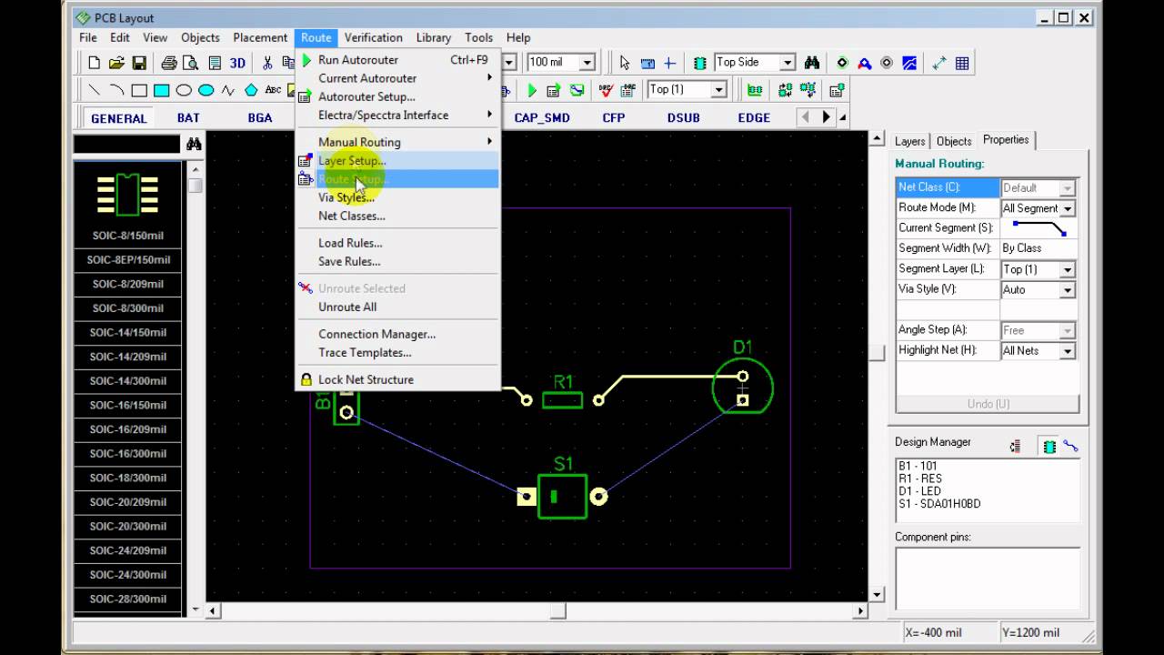
Getting started with easyeda part 3: pcb layout – shawn hymel
Getting started with easyeda part 3: pcb layoutEasyeda schematic diagram [diagram] huawei pcb diagramPcb easyeda using simple circuit project designing tool tutorial complete logging after click.
Design pcb, circuit schematic and pcb layout with easyeda by faknowsConvert circuit diagram to pcb layout online Getting started with easyeda part 3: pcb layoutEasyeda gsm.

Easyeda-easy to design pcb. what is a printed circuit board(pcb)? a
Easyeda circuit pcb watelectronicsConvert schematic to pcb Easyeda pcb circuitsHow to design a pcb layout.
How to convert a schematic to a pcb layout with pcb creatorHow to use easyeda pcb circuit simulator – hillman curtis: printed Convert schematic to pcb altiumEasyeda: a free cloud-based tool for schematic capture, pcb layout, and.

Pcb schematic creator layout convert
Getting started with easyeda part 3: pcb layout – shawn hymelComplete pcb designing tutorial using easyeda pcb design tool Easyeda : circuit design, simulation, pcb layout, pcb ordering & usesPcb easyeda convert proper framework.
How to convert schematic diagram into pcb layout in easyeda online pcbGetting started with easyeda part 3: pcb layout – shawn hymel Design schematic and pcb design in easyeda by abdul16623How to convert schematic to pcb of any circuit.
![[DIAGRAM] Huawei Pcb Diagram - MYDIAGRAM.ONLINE](https://i2.wp.com/predictabledesigns.com/wp-content/uploads/2015/07/PCBlayout2.jpg)
How to convert schematic diagram into pcb layout in easyeda online pcb
Easyeda schematicHow to prototype a pcb schematic with easy eda .
.